ESP32-based heat pump wifi control

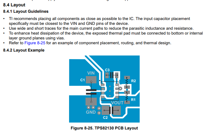
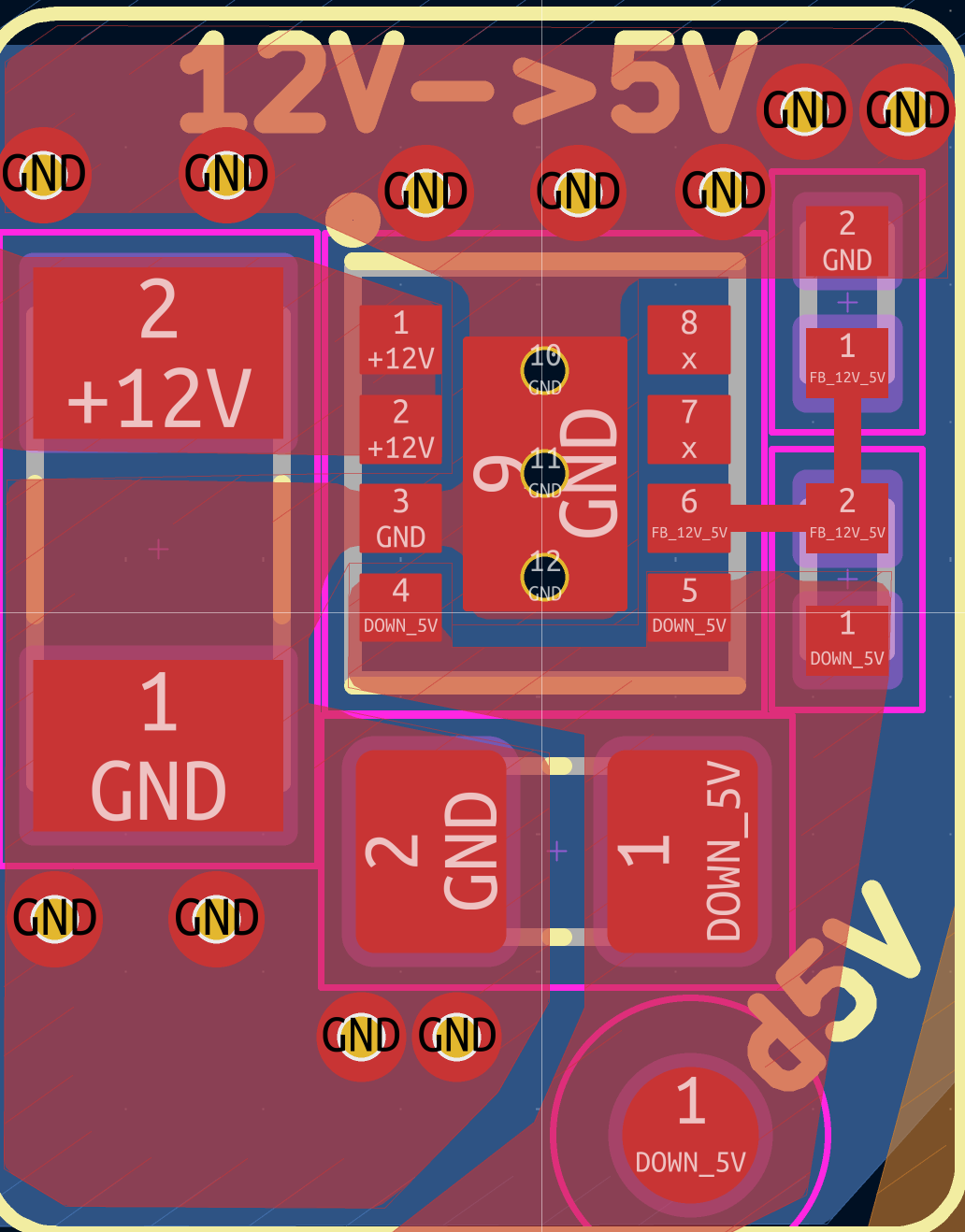
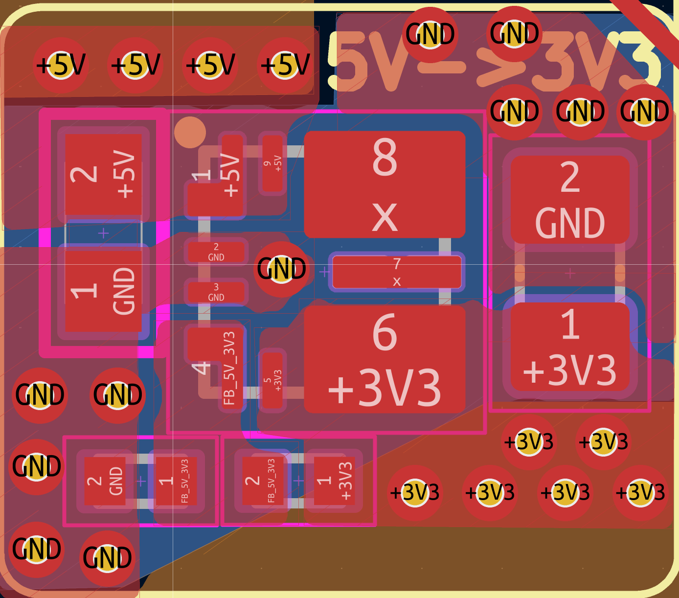
I’d like to control my heat pump’s wall unit via Home Assistant but a separate dongle needs to be bought for each wall unit (I have 3) which is quite expansive. I decided to try to design a PCB and had a lot of fun doing this.

I’m mostly finished but I’m wary of sending it to be assembled; I want to make sure I covered requirements and reduced issues as much as possible before.

For now I mostly concentrate on the hardware aspect. Software will come later.

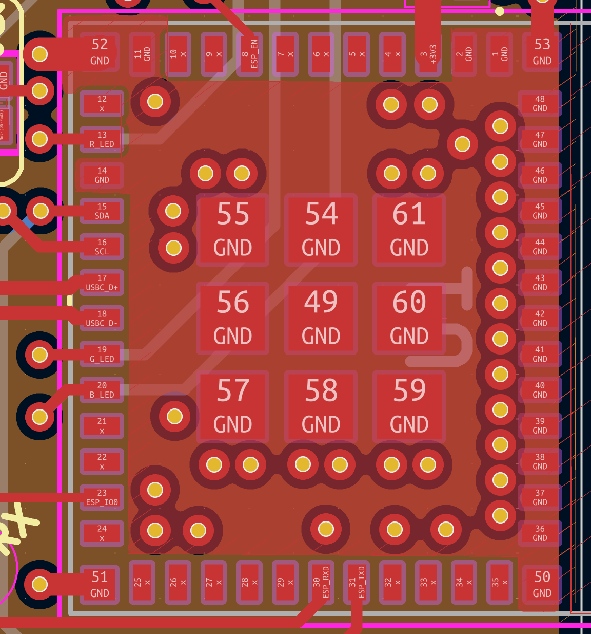
The enclosure where the dongle needs to go is quite tiny (56 x 34 x 9 mm) which constrains a lot the design. That’s why I decided to use a ESP32-C6-MINI-1-H8 for its small size.

All in all I’m quite satisfied but would like to get any second opinion on it. It’s my first PCB design so I might have got some details wrong. I still have some verification to do before sending it to be assembled, but I believe it should work.

I dumped the KiCad files on GitHub here: GitHub - nbigaouette/HeatPumpWifi at v1.0-rc1 · GitHub. There is a rendered directory with images and the schematics in PDF format. I am still writing some kind of README with my goal, constraints, features, etc.

Please let me know what you think!

I would think twice about that little HA looking House Logo.
Should be a lot more different than the official, that might get you in trouble (If you were to sell or distribute)…
image

Good point! I do not plan to selling this, but still. I’ll remove the logo.

EDIT: Done, I’m now using a wifi icon instead.

What brand(s) of heat pump this device is intended to control would probably be good information to include, :wink: especially if it is yet another rehash of the Midea controller…

Hi, I’m not an expert, but there is my assessment based on developing my PCB:

  • 12V → 5V components are placed in different way than recommended by chip manufacturer. My first batch has failed for this reason. There is high frequency switching and good placing of components and GND paths are as important as the right parts itself.
  • 5V → 3V I did not compare it with datasheet, but this one looks better at first glance
  • Temp sensor will be 100% affected by heat of ESP
  • Why “power selector” is needed, if you can not connect both USB’s at same time? Just pass voltage from USB-C directly to 5V in?
  • Which pins will be used for programming and which for external uart? If I understand correctly, TXD0 and RXD0 (which should be used for programming) goes to USB-A female
  • Try to upload your files in PCB manufacturer website and you can be suprised how much they will add for loading the machines with such amount of different components. And I hope you checked stocks of your used parts first, because when I started my board, finally I found out that I used some parts with no stock available and had to do some changes :smiley:

It is quite interesting process to do such boards and receive them assembled, good luck :slight_smile:

My wall units are Fujitsu ASUH12KPAS and ASUH07KPAS. So, not Midea :wink:

1 Like

Thanks @Benas, that’s awesome feedback! I’ll review every points for sure.

  • 12V → 5V: I will double check the components placement. What problem did you see more specifically?
  • The power selector’s role is to prevent voltage/current flowing back into the other connector. When the device is powered by the USB-A connector it’s not a big deal; the USB-C power pin will be brought to 5V but there is no circuitry. But when the USB-C is connected and powered, the 12V → 5V will see 5V on its output pin and I did not want this to affect the components. I initially though a jumper header would be sufficient, but it made things more complicated than just having an IC. I settled on the TPS2116DRLR as it was simple enough. Do you think this is not required?
  • The USB-C is used for programming. On the rendered board, test pins D+ and D- are available (one pair before and one after the 5V TVS diode). They are connected to the ESP32’s pins 17 and 18 (GPIO 12 and 13). See datasheet page 11, table 3.1, page 11. In there those pins are identified as USB_D- and USB_D+, which I believe is what is required for programming.
  • For external UART, the tests points are identified as TX and RX. Those test points appear after the TVS diode and voltage shifter, so they are 3.3V. The RX test point connects to ESP32’s pin 30 (RXD0/U0RXD in the datasheet) and test point TX is connected to ESP32’s pin 31 (TXD0/U0TXD in the datasheet). The USB-A receptacle’s pin 2 and 3 are AC_TX and AC_RX, respectively. AC_TX connects to RX and AC_RX to TX. This is quite confusing for sure, and I will re-tripple-double-check those connections.
  • I did upload the design to different manufacturers to get quotes (PCBWay, NextPCB, JLCPCB). PCBWay complained about the level shifter which was too small (TXS0102DQMR). I changed it to the larger package TXS0102VDCUR. I was also previously using 0201 components, which are too small. The smallest components are now 0402, making it easier for manufacturers.
  • I harmonized the components to reduce their count as much as possible. For example there is seven 5.1kΩ resistors and five 0.1μF capacitors.
  • JLCPCB had the best experience overall, but unfortunately it does not have some of the components. I will probably fallback to PCBWay which did not seem to complain about non-available components. Digikey does have every one of them in stock though. But yeah, I might have to do some changes due to this.

I’ve learned a lot doing this and it was really fun! I’ll be super happy when they finally arrive, but I for sure want to minimize any possible error.

Basically you have copy this layout for components placement and track (copper regions) routing Otherwise you risk unstable VOUT, overheating.

  • In your layout there is long route from Vout cap to voltage divider (it matters when there is high frequency switching).
  • Vin and Vout capacitors are far from each other, in different sides of IC
  • Too small GND areas will not help to cool down the chip efficiently

When you will give 5V to USB-C, the most that will happen (I think) - 12V stage output capacitor will be charged to 5V.

I did not know yet that C6 mini has USB controller included, nice :slight_smile:

Thanks for the details. I’ll double check and try to improve the design.

Regarding the power selector… I don’t think it is ok for a voltage to be applied to the TSP82130’s VOUT and FB pins, even when the device is not enabled or driven by 12V on its VIN pin. So something has to block current/voltage from the USB-C’s power from flowing back into the TSP82130. I did asked about this on the TI forum so we’ll see if I’ll get a reply and what kind of information will be suggested.

I do remember now why I picked up the TPS2116 power switch. First approach would have been to use a Schottky diode. The diode has a voltage drop though. It’s not large, but it’s not negligeable either. Components details mention up to 0.5V, but looking at curves in data sheets it seems it can go up to 1V. The TSP82130’s output should then be adjusted to cover this loss. But worse is that the diode would heat up under normal use. This is wasted energy. And the smaller the diodes are, the less efficient they are. They also have lower current ratings which could be problematic.

The next solution was a MOSFET. But those require extra components which complicates the design and increase the cost. And this is a manual solution; I needed to select all parameters properly. This was more complex then using a Schottky diode.

Then I found the TPS2116 from Texas Instruments. It’s basically some MOSFET packaged properly for that exact use case. For the same package size, it provides exactly what the need is here; select one power input only. It even support having both power source connected at the same time (it will pick up one over the other according to how the resistances are connected). Because of its switching nature, there is basically no loss (a 40 mΩ resistance). Power loss can be 4 times smaller than a diode.

When looking at the price, the TPS2116 is more expansive for sure, but it’s not too bad compared to the rest of the system. So I think it’s worth it.

I’ve updated the layout to follow more closely the TPS82130’s suggested layout:

  • The capacitors are now placed similarly to the data sheet
  • There’s now a ground copper zone covering the underneath of the IC with thermal vias, hopefully that should be enough for thermal dissipation…

Looks better. You can make GND areas even bigger (fill all area defined for 12 → 5) add more holes (called stitching) and create same size GND area in bottom layer. It will suck the heat. Also check layout for 5 → 3. It looks better but possibly also can be improved.

Fb is connected through voltage divider, so it will get 0.9V or something similar, it is feedback for regulation of Vout. When chip is shutdown it should do nothing. Of course its good practice to conslut with the experts what you did in that forum :slight_smile:

I got an answer from the TI forum:

Applying 5 V to Vout with VIN = 0 is generally safe for TPS82130 since the output stage is high impedance in shutdown.

If that’s the case then I’ll probably remove the power mux IC. With it, both USB port could be connected/powered but it’s probably not worth it.

Regarding the 12V->5V region, I added a copper zone on the last layer covering the region itself and up to the mounting point on the left. From what I understand, stitching vias are meant to connect two layers of the same net to prevent EMI. They can also be used for thermal dissipation. When you suggested them, were you concerned of the EMI due to the two ground planes? There’s not much space for vias near the IC. Here’s what it looks like (the blue zone is GND on layer 4):

For the 5V->3V3 region, I’ve re-arranged the components to be closer to the datasheet’s layout example. I also added a GND zone on layer 4.

It’s hard to evaluate the thermal effect of these changes. To do so I’ve used this plugin: GitHub - PoeAlex/KiCad_Thermal_Sim: Fast Multi-Layer Copper Thermal Estimator for KiCad · GitHub . I’ve used it not for its absolute value but to check the effect of the changes I make to the layout. I select pin 1 of either the 12V->5V or 5V->3V3 IC, and keep default parameters (1W, 20s, 25C, 0.46 mm). Initially, I had 62.9 C maximum for the 5V IC, and 74.8C for the 12V IC.

Re-arranging the 12V components the max temperature increased to 83.5C. Adding the GND zone on layer 4 under the 12V region brings the temperature back down to 63.6C. I did not see must effect with the number of vias.

For the 5V components rearranging the components more closely to the datasheet layout rises the temperature to 72.3C. Moving the TPSM828302 a bit up closer to the 5V vias brought it back down to 64.8C.

So my conclusion is that moving the components more closely to the datasheet layout increases the temperature, but adding the GND copper zones on layer 4 bring it back down to what it was initially.

I’ll play around with the vias to see find the minimum amount that makes sense (thermally).

I’m wondering if the ESP32’s vias are fine? I don’t think vias should be placed under the nine GND pads, so I placed them around the pads. Anything to say about this? :thinking:

Interesting plugin and observations.
As I said, I am no expert :slight_smile:
I think that plugin does not take into account the fact that the wrong layout will generate a lot more heat and it compares how the same amount of heat would be dissipated.

Vias connect two planes which each other and conducts the heat between them (like water pipes in heating system). So when you connect both planes you basically make your “radiator” twice as big.

For ESP32 vias, it looks like that they are separated from the GND plane in their own island