Want PCB replacements for Google Home Mini and Google Nest Mini to run ESPHome firmware and be based on the same ESP32 + XMOS chips as Home Assistant Voice Preview Edition!?
Are there any PCB (printed circuit board) engineers/designeers this community with time and interest to design and build PCB schematic for new DIY custom ESP32-based third-party alternative circuit-boards for the Google Nest Mini and Google Home Mini (smart speaker devices) that will work as drop-in PCB (Printed Circuit Board) replacement boards similar to the old Onju Voice project but be designed to use a newer updated design that also adds an XMOS-chip (advanced DSP connected to the microphone for voice quality cleanup) to match the more modern hardware specification of the Home Assistant Voice Preview Edition as well as have a fully free and open-source hardware design?
That is, it does not seem like justLV will return to continue developing his onju-voice PCB design to add an XMOS chip, plus the fact that the original project was never being made into a fully open-source design without restrictions I was wondering and hoping that some other talented electrical engineer(s) with PCB design experince will step up to make some new PCB designs for the same concept + publicly release all that as fully open-source PCB designs and schematics that has a similar concept as the Onju Voice project but instead being made as a fully open-source drop-in replacement circuit-board for Google Nest Mini / Google Home Mini (smart speaker) series and also using the same ESP32-S3 but adding XMOS xCORE chip same as the new Home Assistant Voice Preview Edition reference hardware from Nabu Casa?
So essentially an new custom open-source circuit board for converting Google Nest Minis into Home Assistant Voice smart speakers:
As most of you probably already know; Nabu Casa development team together with other ESPHome and Home Assistant core developers have made progress by leaps and bounds over the last year and with the release of their official Home Assistant Voice Preview Edition reference hardware.
The concept of the Onju Voice drop-in PCB replacement is at least in theory showing more promise than ever and better user case for a larger audence, its lack of an XMOS DSP MCU chip and missing dual I2S bus makes the current PCB design obsolete as that the improved user experience you get with the XBMOS chip added is a night and day difference:
The optimal goal would be a PCB design that anyone could make themselves or order pre-assembled PBC-replacement-boards for Google Nest Min (and Google Home Mini) directly from PCB-manufacturing-service such as for example PBCWay, OSHPark, or JLCPCB, that offers “shared projects” community designs, (hence wish for an open-source license without commercial restrictions clause), that will enable people to re-puropse their existing Google Nest / Google Home smart speakers within their enclouses.
There are already huge stock of those out there and users who might be incline to migrate on a budget can be willing to thinker with such a project of such a PCB is designed released by electrical engineer(s) with the skills, time and interest to make this happen.
Any one here perhaps got contacts at any one of those PCB-manufacturing-services that might be willing to run and sponsor a contest or similar effort to speed up such a development effort?
PS: Slightly off-topic but be aware that many Amazon Echo users have requested the same, see:
And of course, once I have done the schematic, then we can transfer that to other PCB shape to fit in Echo dot for example. The only thing is my main goal is to repurpose my Nest minis, as I never really had any Amazon smart speaker.
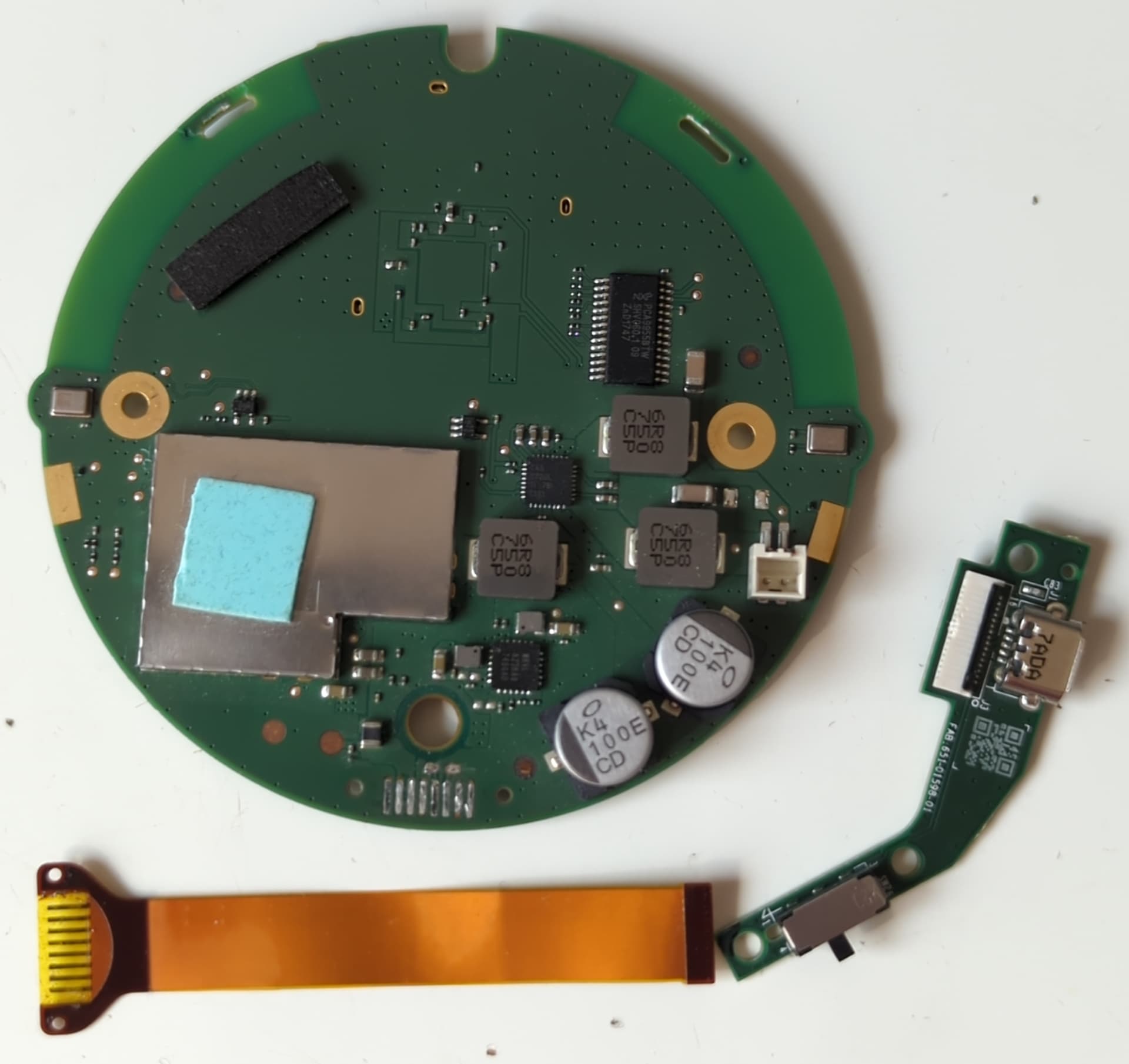
Okay, so this is roughly how it will look. All the schematics are done, and the component placement is finished (although it might change slightly during routing). At this point, I could really use some help from someone with experience in GND pouring, shielding, and overall routing. I can handle it myself, but it would probably take me a few weeks, and the next two weeks will be quite busy for me. So if anyone is able to help speed up the process, I/we would really appreciate it.
By the way, what software/applications and formats are you using for PCB layout and schematics?
Edit: I also think it might help if you could upload everything in-progress to a new repository on GitHub so those interested can review and evaluate the complexity, etc. so know if they can contribute or give feedback.
PS: Wondering if there are any AI-tools out there yet that can assist with such PCB design tasks such as GND pouring, shielding and overall routing?
Thanks a lot for your suggestions, much appreciated!
I’m using KiCad for both the schematic and PCB layout. It’s been working great so far, especially with the 3D integration for enclosure fitting and placement accuracy.
Regarding AI tools — while there are some experimental solutions out there, currently there’s no truly reliable AI-based tool that can automatically handle complex tasks like GND pouring, shielding strategy, or full routing. They can assist (e.g., suggest net classes or analyze potential EMI hotspots), but human input is still absolutely required, especially for audio-focused or noise-sensitive designs like this.
And yes, good idea about uploading the in-progress files to GitHub — I’ll definitely prepare a public repository soon so others can review the current state and possibly contribute. Thanks again for the suggestion!
Here is my repo
I’ve also added a license specifically for the hardware: CERN-OHL-S v2 — a strong copyleft license that ensures all derived versions remain open source as well.
PS: happy to answer questions or accept contributions
Recommend you check if could use the same license for the hardware design files as newly released “Home Assistant Voice Preview Edition” (also known as Home Assistant Voice PE) If it is possible:
Oh, I forgot to mention this idea to better future-proof the design; and not to go away too much from the original topic, however if you would like to make the PCB layout design more future-proof then you should probably consider leaving room on the board to also add a second ESP32 on the same PCB.
Specifically I think that it would be awesome to also add an ESP32-C6 as “coprocessor” and “IEEE 802.15.4 radio” module to future voice boards, (meaning making a single PCB that have both a ESP32-S3 SoC and a ESP32-C6 SoC on the same board), so that second SoC can be used as dedicated Thread Border Router radio module.
Thanks for the suggestion, I really appreciate the input!
However, I plan to stick closely to the original concept of the project, which doesn’t include a touchscreen or a Thread Border Router. My goal is to build a compact, streamlined board based on the existing HA Voice PE design, and at this stage I don’t intend to add extra components like a second ESP32.
The PCB is already quite packed, and considering the current complexity — especially without external help — I’d prefer to keep the design as lean and focused as possible.
This project is licensed under CERN-OHL-S v2 (Strongly Reciprocal), which is specifically designed for open-source hardware. It’s different from the Home Assistant Voice PE licensing model, which uses GPLv3 and MIT — both of which are better suited for software and firmware.
We intentionally chose CERN-OHL-S v2 because it ensures that any distributed modified versions of the hardware must remain open and licensed under the same terms. This protects the open nature of the hardware itself, much like GPL does for software.
Unlike MIT (which is permissive) or GPLv3 (which isn’t tailored for hardware), CERN-OHL-S v2 provides a legally robust framework specifically for PCB and hardware reuse, which better matches the goals and structure of this project.
It’s also widely recognized in the open hardware community and supported by platforms like KiCad and the Open Source Hardware Association (OSHWA), making it a natural choice for a community-driven hardware design.
The goal isn’t to throw a house party — for a voice assistant, 3 W is more than enough.
The audio quality will already be significantly better than on the HA VPE device, and it’s perfectly capable of handling music playback as well.
I have both device, but for now the Nest mini V2 is the main device. I don’t think the two PCBs are identical, but I never checked that. Anyway, as the schematics are done, we can make any other PCB design and placement later. Other option is, free to use for anyone who is capable to make one.
Regardless if possible or not, what would complicate such an idea is that it should really be able the power-supply that shipped with the product. That is, Google Home Mini (Gen1) ships with a Micro-USB changer as power-supply while the newer Google Nest Mini (Gen2) ships with a custom barrel-jack power-supply. It would add to the total cost of the device if you not only need to replace the PCB but also the power-supply, (as at that point you might as well just try to buy a used Google Nest Mini Gen2 instead of buying a new power-supply too).
PS: On a personal note I actually only own a single Google Nest Mini (Gen2) today, while I also own six of the Google Home Mini (Gen1), …as well as two original Google Home (pinapple), and two Google Home Max + two Google Nest Hub + five Chromecast Audio.
I do not know the answer but agree that you would want to have the best possible amplifier suitible for the use case of using it both as a voice assistant and
While it is obviously not meant to be a dedicated party speaker, I have to add that the original Google Home feature of pairing two of them in stereo-mode for use in a single room makes for a good enough music speaker, (and personally I do actually use them for house parties too as I have at least one in each room and even two in some rooms ).
Yeah, we are not the same, that’s true. For house parties I like to use something more powerful like my Marantz Cinema 50 with heos.
I have used the MAX in other custom built smart speaker project, and while they are not a power horse, still quite good quality, and enjoyable
I’m glad that I saw this thread. I was just about to order the original board design on PCBWay. I have a couple of old Nest Mini 2nd Gen that I no longer use, and I would like to convert them to HA Voice devices. Thank you for updating the board design!
OK so I’ve been watching this thread, but I am a little confused. Is this design ready to go? Should I be ordering some or are we waiting for a few more edits?
They are different but maybe in the future a version can be made to fit both.
As @Hedda already wrote they are powered differently but imo a Gen1 has the benefit that it could be flashed without opening it.
And also the chance that Gen1s go EOL is higher ^^