COSTCO FEIT/Tuya-based WIFI Dimmer - Step-by-Step Guide (Newbie friendly)

As the original COSTO FEIT Wifi Dimmer thread has become quite long and has many branches of topics, this thread will attempt to capture the basics of converting these Tuya-based switches for those that can no longer use the exploit that Tuya-Convert used. If you have old switches (pre-mid2020), you should first try Tuya-Convert because that will be MUCH simpler than these steps.

Before we get started with the step by steps, a few WARNINGS, CAUTIONS and NOTES

WARNING - you will be dis-assembling a device intended to be connected to 120V mains. Electrocution is a real possibility if you connect your device to your AC main power while it is open. Don’t even consider removing the first screw if you do not understand the shock risk involved. The author of this thread assumes no responsibility for your personal safety should you decide to follow the process being documented. This is what the author did - not what you should do.

WARNING - if you ignored the first warning, realize that the low power (5/3.3V power supply) within this device is not isolated from the 120VAC side. It “floats” and even touching a low power trace on the DC side could result in a deadly electrical shock if you are sufficiently “connected” to ground or common wiring on the mains side while connected to 120VAC Mains.

CAUTION - this project involves delicate and tedious de-soldering of printed circuit board components. Too much pressure or heat can permanently destroy components on that board and render the entire switch useless. If you are unwilling to potentially sacrifice one of your switches (or two) as a learning experiment - TURN BACK! If you destroy the pads and/or traces on the Tuya board, it is pretty much game over unless you want to source a new TYWE2S from China or try to hack in another ESP8266-based board into the switch.

NOTE - Ideally you would have a SMD re-work station like these. If you are reasonably talented with a soldering iron, you can get this chip off the board without destroying it - but it will not be easy. (This is a NEWBIE thread - so for those who want to say it is no big deal - I refer you to the thread title! :wink: )

NOTE - this process will liberate your device from the “tyranny” of manufacturer’s cloud controller and allow you to integrate it into your own automation solution. But it goes without saying, you now own it fully. No warranty (please don’t bork a PCB, reassemble it and take it back to Costco claiming "it doesn’t work…) and no support other than “asking the internet” and hoping people will be kind enough to guide you through the steps to fix it.

NOTE - this guide is going to presume you will use ESPHome as an Integration within Home Assistant. There will be code examples in subsequent posts to make this device work within HA and using ESPHome. If you prefer to go the Tasmota route, follow the hardware guide until it is time to flash the chip… and then start your own NEWBIE thread!


OK - enough discouragement. You are here to make it work!

This Step-by-Step DIY guide will break the process down into 5 areas:

  1. Disassembly and prep for de-soldering work
  2. Desoldering process
  3. Prep for flashing
  4. ESPHome code and flashing
  5. Reassembly and testing

Since it is intended to be a detailed guide, each step will be a new post. The first 5 posts in this thread will be the steps. Discussion can then continue with reference to POST#2, 3, 4, 5, or 6

5 Likes

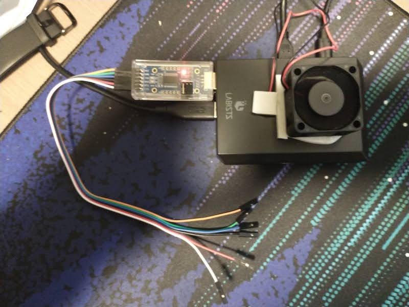
STEP 1 - Disassembly and prep for de-soldering work

The switch has two primary sub-assemblies. The top (white) part which contains the printed circuit board (PCB) that we will need to work on, and the bottom (black) part that contains the 120V AC Mains circuitry and low voltage power supply. We will not be doing ANYTHING inside the black housing.

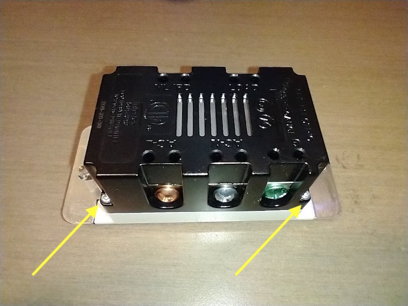
Flip the switch over and remove the 4 screws (pic with arrows) with a small Phillips screw driver.


The black base separates from the white top. Before you start pulling, realize that there are 8 small pins that connect the lower base to the upper switch frame and PCB. See picture. When you pull, you need to pull straight out and slowly so you do not bend the pins.

We will not be doing ANYTHING with the lower half until reassembly. You can set it and the 4 screws aside (don’t lose the little screws.)

We now need to take the PCB out of the white switch housing. It is held in with 3 even smaller Phillips screws. Once removed, the board will simply fall out of the white housing.


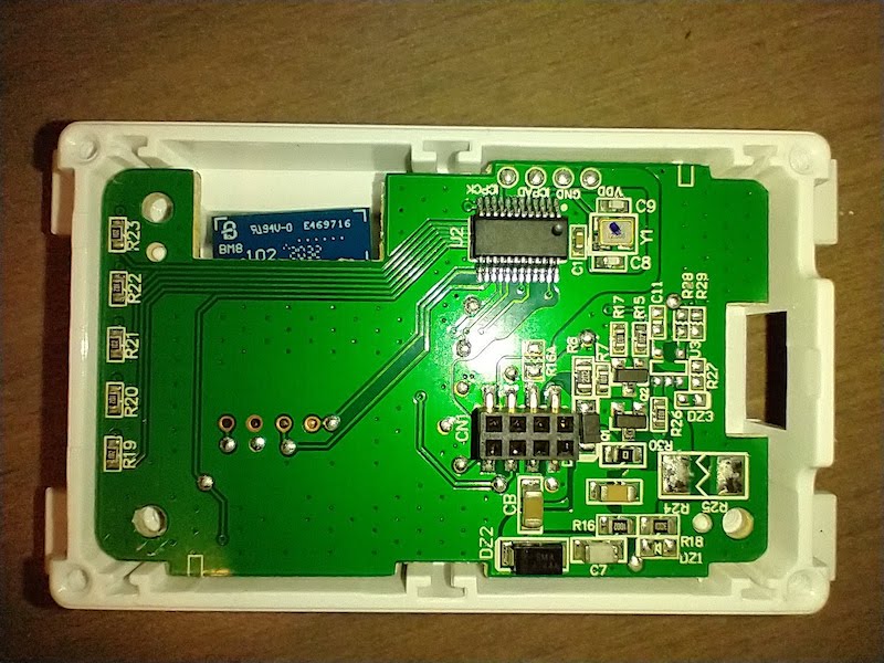
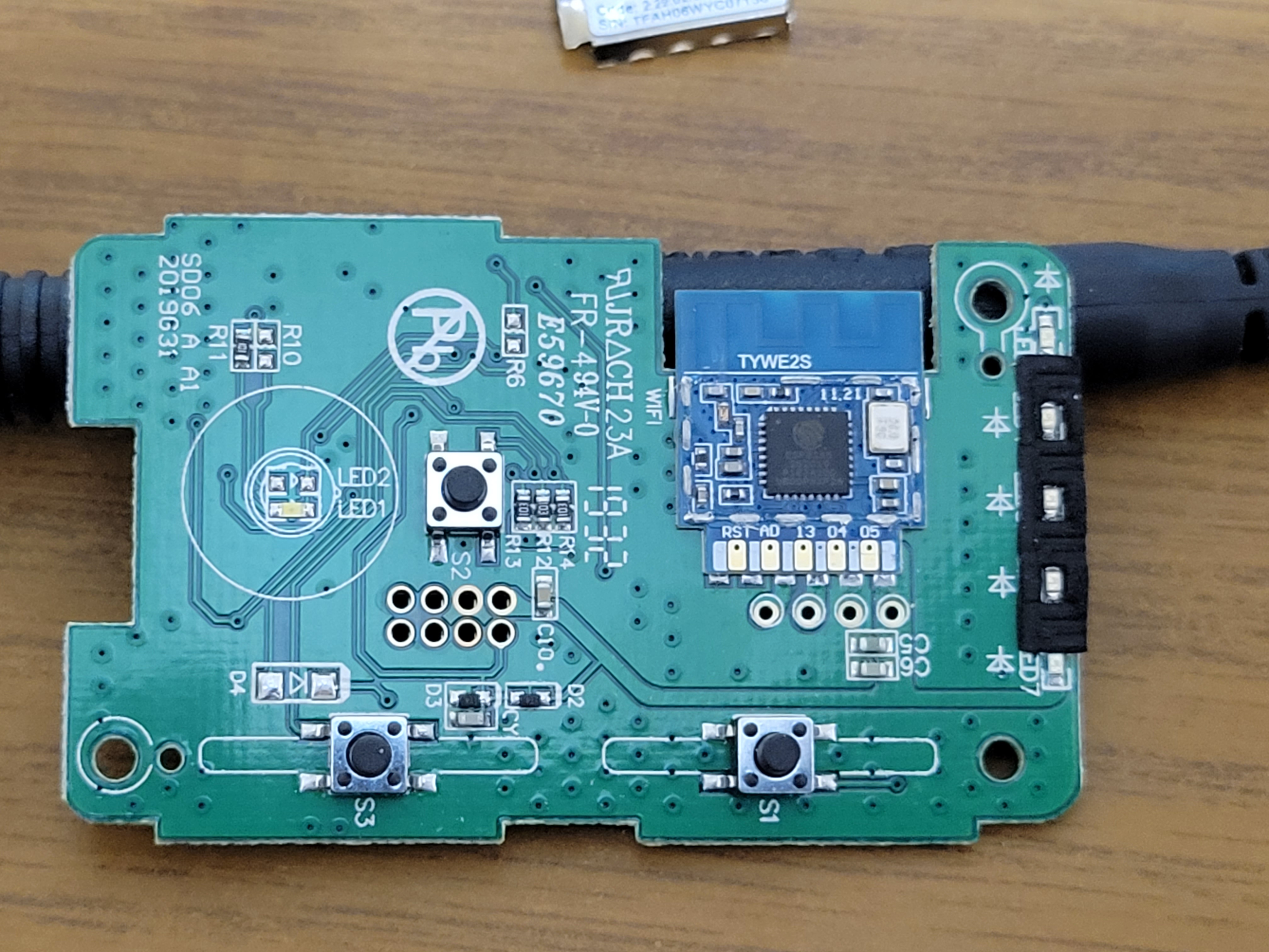
Before we jump into desoldering, lets do a quick orientation on the PCB.


A - this is the Tuya TYWE2S (ESP8285) wifi/microprocessor module. The wifi radio, cpu, flash memory, and input/output circuitry is all inside that metal shield. This is where our ESPHome firmware will all live and where any customization will happen.
B - these four holes are test pads that could be used to re-program the ESP chip. They are in fact connected to 4 of the 6 pads that are soldered down across the front of the board. In the picture they are:

  1. VCC - 3V3 (Positive 3.3 VDC) power to run the chip
  2. Ground - common to the whole board (and NOT connected to AC common or Earth Ground)
  3. RX - The RECEIVE side of the serial (UART) communications TO the ESP FROM your flash connection
  4. TX - The TRANSMIT side of the serial communications FROM the ESP TO your flash connection

In fact we are not going to use those pad until testing later. But describing here for completeness. The rest of the labeling is just for your education. We will not be doing ANYTHING with any other component on this board.

C - the dimmer level LEDS (green). Controlled by the MCU.
D - the ON/OFF switch. It does not turn the power on and off. It sends a signal to the MCU.
E - the dimmer up/down switches. Same thing. They are just signaling devices to the MCU.
F - the ON/OFF switch backlight. Controlled by the MCU.

G - the MCU - microcontroller unit. This is a custom-flashed chip from Tuya that actually does all the work in this switch. It turns LEDS on and off. It listens to the switches above for commands. It sends signals to the circuitry in the black housing to actually turn the AC Mains on and off and dim the AC lights. It reports back to the TYWE2S the status and listens for requests from the TYWE2S to make changes to the light.

Think of the TYWE2S as the wifi “brain” that allows the Internet of Things to talk to the MCU. The way this switch/board was built, the TYWE2S doesn’t do much other than relay the conversation from the network to the MCU. Not all switches work this way. Some will have the ESP device controlling aspects of the board directly. The MCU is a bit of a black box. We can talk to it from the RX/TX lines and tell it things like “Turn on the light” - but it has to do the work of actually opening or closing the relay. So we are limited in how we can “get in the middle” and do more advanced controls with this switch.


Before we start actually de-soldering, lets talk about WHY we are de-soldering.

In order to “flash” this ESP with a new set of instructions, we need to make 5 connections (not 4).

  1. Power
  2. Ground
  3. RX
  4. TX

OK - we have all 4 of those right there on the board and could just push some board jumpers into the hole - right?

Well - not so fast. We have to put the board in a “state” that it is ready and willing to be flashed. Otherwise it thinks it is in a conversation with the MCU. AND - if we connect those 4 pins, the MCU will be powered and the two devices WILL be talking to each other.

In order to get in the middle of that conversation, we have to a) shut-up the MCU so it doesn’t talk and b) tell the TYWE2S to be “ready” to accept a new program.

We might be able to accomplish a) by holding one of the pins on the MCU to ground or holding it “high” to 3V3 - but in this case, that doesn’t help us because we need access to a special pin on the TYWE2S that makes it ready to be programmed.

Whether intentional or coincidence - this board has the pad to do that on the back…

Lets take a look at the TYWE2S in detail. And also - lets stop referring to it by its chip name and just call it the ESP as shorthand for the ESP8285 chip that is inside - which is VERY similar to an ESP8266 which you will hear talked about a lot in the IoT world.

Anatomy of an ESP (8285)
TYWE2S-Front
(Photo credit - poster Skysoft from this forum.)

A - this is the wifi antenna - which explains the cutout in the main PCB to give better wifi signal strength.
B - front side pads (none of which we will be using for this project - but we must be careful to not create a solder bridge to later)

B1. RST - hardware reset pin. Won’t help us for this project
B2. AD - Analog to Digital conversion port
B3. 13 - General Purpose Input Output (GPIO) #13
B4. O4 - GPIO4
B5. O5 - GPIO5

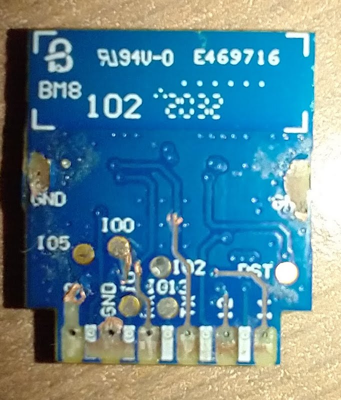
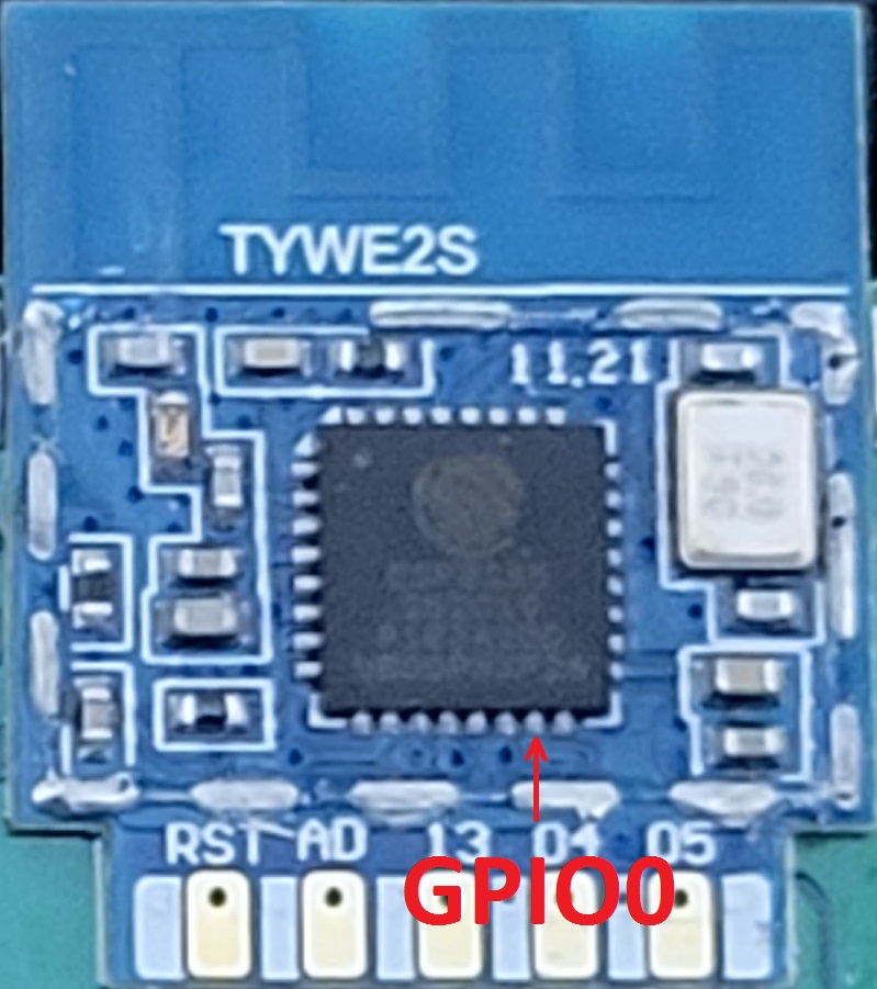
On the back is the “business” side of the chip we need.


(Photo credit - poster Skysoft from this forum.) I don’t have a “good” ESP dismounted at the moment. Next post will show what a botched desolder job looks like)

  1. 3V3 - VCC - Positive 3.3V power input
  2. GND - Ground (logic ground - not earth grond)
  3. RX - UART0 Receive (the “listening” end of the serial interface with the MCU or our flasher)
  4. TX - UART0 Transmit (the “talking” end of the serial interface)
  5. 12 - GPIO12
  6. 14 - GPIO14
  7. I05 - GPIO5
  8. IO0 - GPIO0 (yes - that is an “OH” (O) next to a Zero (0) - and this one is important!
  9. IO4 - GPIO4
  10. IO2- GPIO2
  11. IO13 - GPIO13
  12. RST - Reset (again)
  13. GND - Ground (again) and attached to the metal box.

Amazing little bit of kit. An entire microcomputer, memory, wifi radio, and serial modem all smaller than a postage stamp! And also a big pain to work with since it is soldered down completely underneath the board and has very delicate traces and pads.

Why do we have to remove it?

Because we have to have access to #8 above. GPIO0. This little solder pad is the magic to make everything happen. How we will use comes later - but we have to gain access to this pad to do everything else. Before you ask - No, you can’t just drill a hole in the main PCB. No, you can’t somehow slide a wire underneath. No, there is no easy way around this. (Or if you are brilliant enough to figure out how to do this without removing it from the PCB - you shouldn’t be reading this newbie thread!)

If you now feel daunted by the prospects, thanks for reading this far - and good luck with another brand of switch.

But if you want to learn something - or are unaware of the Fallacy of Sunk Costs - or are unaware that you could just take these switches back to Costco (BEFORE you’ve taken it apart and broke it) - FORGE AHEAD. It will be frustrating, nerve-wracking and … oh yeah … fun too!

1 Like

Step 2 - Desoldering Process

I won’t pretend to be ANY kind of expert on soldering / de-soldering. I’m going to relay what didn’t work and worked for me. Others are free to chime in and share technique that works for them.

Before we jump into doing the work - let me show you what happens when you either don’t know what you are doing or get impatient and use heavy hands.

I’ve botched 2 of 10 switches myself from inexperience and impatience.

The solder that is used at the factory has no lead (Pb) in it. Consequently it is VERY strong and has a high melting point. For us that spells “hard to remove.” It doesn’t “flow” as well and consequently, even when it melts, it has more structural bonding than 60/40 PB/SN solder.

The pads and traces are very delicate and if you start tugging before the solder is ready to let go, they will pull away from the PCB and ruin it for further use.

For all to witness - here are my two examples of what not to do…


What do you need?

Well - you can probably do all of this with just a soldering iron and some solder wick - but I don’t have that talent. What I used was the following:

  1. A SMD rework station (has both a temp controlled soldering iron AND a temp controlled SMD hot-air tool.)
  2. A set of “extra hands” to hold everything while I worked.
  3. 60/40 PB/SN solder (mine is rosen core 0.6mm “fine”)
  4. Narrow solder wick (2.5mm width is what I had. 2 would have been better)
  5. No-clean flux (I used a flux pen)
  6. Some sort of thin metal “spatula” for prying and getting under the ESP as it starts to lift from the board (I had several tool kits with various metal tools - you need metal or you will melt it!)
  7. This is small work. Unless you very good close-work vision, I recommend a magnifier of some type. I wear a headset with interchangeable lens. (I wear 1.25 readers to work at a computer and 1.5 readers to read as a point of comparison. I did most of this work with the 2.5x lens in my headset.

I’m not going to do a soldering/de-soldering tutorial here. Just touch on some basic technique that worked for me.

  1. I started by using the helping hands to hold the PCB.
  2. 330C on my gun and my iron seemed to be a pretty good spot - maybe 345 for the ground points. In theory the lead-free solder melts at 220C but you have a lot of mass around the pads sucking your heat away. I did scorch some boards with higher temps when I started. Nothing that didn’t work but better to use the lower temps and patience - at least for me.
  3. I heated the back of the PCB below the ESP with the gun for a while to get the entire ground plane and PCB substrate hot so it didn’t wick my heat away so fast. Others say they successfully were able to dismount the ESP with just backside heating and gentle pressure - but I never made that work.
  4. After general heating, I flipped the board over, applied some flux from my flux pen at the ground joints and wicked away solder as best I could from the two ground points using my iron. Remember these ground points are attached to the large ground plane of copper underneath the coating on the board - so the heat dissipates fast.
  5. After I wicked away some of the lead-free solder, I added back some PB/SN solder so that it would flow under the board a bit. This gives better heat transfer and hopefully alloys with the lead-free a bit.
  6. I then re-heated the reverse with the gun again.
  7. Working on the ESP side with my gun aimed right at the joint, I let it heat for a while. The solder holding the metal shield to the ESP may actually start to flow - which tells you the ground solder is getting there as well. Don’t worry, we aren’t going to pry on the shield, so it isn’t a problem.
  8. With the ground solder starting to flow, I put my metal spatula in the gap between the PCB and the ESP wifi antenna area and left the handle sticking out to the side so the weight of the tool applied upward pressure on the ESP - WHILE still applying heat with the gun.
  9. I found the ground points would “creak” a little as they started to separate. You may need to remove the heat with pressure on the joint - and work the opposite side. You will likely end up with two narrow solder bridges still connecting the two boards. THIS IS WHERE IT GETS DICEY.
  10. You only want enough upward force to just break the bridge. You are not trying to completely lift the board because it is still firmly attached at the front pads. In fact, I frequently re-applied heat to the front pads to allow the solder in that area to relax and start to separate so I didn’t tear them (after my first mistakes.)
  11. Once both ground joints are separated, you may want to slide a thin tool in between the two PCBs so that they do not re-bridge.
  12. Finally we can work on the front using the same general procedure - except that we really need to get all 6 of the pads in front to flow at the same time. What worked best for me was to push against the front of the ESP (trying to slide it towards the ground points and the gap in the main board. Horizontally.). With this technique the 8 success stories just sort of popped off all of a sudden with no pad tears.

For “pro” lurkers who actually read this thread - I WELCOME any technique hints you may have here. This is just what worked for me.

Once the ESP comes away from the main board, use your solder wick and iron to clean up all of the factory solder.

I don’t have any pics of the process because I wasn’t documenting as I went. Putting this tutorial together after the fact.

Step 3 - Prep for Flashing

Congrats! You got the ESP off the main board without damage and all fingers are intact without burns! (I hope.)

Before we can flash, we need to prep and need some tools.

Still having all of the tools at hand from the previous step, I added in some jumper wires. If you some already, great.

If not - here is what I did. I pulled all of the conductors out of a 1 foot (30cm) piece of CAT6 solid core 23AWG wire. Now I have 8 conductors with different color codes so I can keep it all straight.

For flashing, I created 4 short (2 in / 5cm) jumpers - each a different color. On one end, I stripped about 3/8" (10mm) of insulation and on the other end about 1/8" (3mm). The long end will be inserted into the female Dupont connectors for our flashing device. The short end is getting soldered onto the ESP.

I had one longer wire 6" / 15 cm that I gave the same treatment.

The 4 short wires will get soldered to the 3V3/GND/RX/TX pads and the long wire to IO0 - but more on that in a minute.

If you haven’t already, clean up the pads on the ESP, flux and apply a small bead of solder to each of the 4 pins (3V3/GND/RX/TX). This will be easier than trying to flow solder onto the wire and pad at the same time. Also apply a bead to IO0.

We are soldering wires to the following pads as labeled in this picture: #1, #2, #3, #4 and #8

Now we attach one short wire to each of the 4 pads already mentioned with a brief touch of the iron to the wire sitting on top of the solder bead on the pad until it melts into the bead. Hold steady until the bead cools. Then be VERY careful you do not push on this wire as you can tear the pad away even with the leverage of the copper wire.

At this point, you need to have the ESP held steady somehow because you will be soldering the long wire to the IO0 pad and it is easily torn off. I bent this long wire in advance before soldering. The wire will need to touch the nearest grounding pad (#13 on the left in the above picture) when you apply power to the board to signal “flash mode.”

You could do this without soldering to IO0 if you have a steady hand - but for me it was easier to bend the wire so it would naturally touch both IO0 and the ground pad and then just tack it on with solder.

Congrats - you are almost ready to flash. 4 short wires ready to be inserted into the Dupont connectors of your UART module and a long wire that will be used to ground out IO0 when we apply power.

At this point - you will need SOME WAY to communicate with the ESP.

I personally am using a FTDI UART module that plugs into the USB port on my Raspberry PI4. This is easier for me than trying to deal with the pins inside the RPI. But you could just use the RPI (can’t help you with that - I haven’t done it. But if you don’t have a UART USB connector and DO have an RPI - then that is the way to go!)

Here is my “flashing” rig.


This FTDI module has a jumper on it that allows me to select 3V3 or 5V for the VCC pin. You need 3V3 and can potentially damage the ESP if you apply 5V.

You don’t want to get in the habit of connecting and disconnecting pins while there is power applied (another reason I don’t want to use the pins inside the PI.)

I “dry fit” my setup by turning off the RPi, plugging in the USB, mounting the ESP in my helping hands with the short wires pointing towards another helping hand. Then I put the connector end of the ribbon cable in a helping hand to hold it steady and make sure I can mate all the soldered wires with the pins without any tension on the soldered wires (so I don’t tear off a pad.)

Sorry - no pic at the moment of this setup - but there are some pics in the main COSTCO FEIT thread that will get you headed in the right direction.

In the next post I will discuss the actual software to perform the flashing - just getting all the physical bits in place at this point.

Step 4 - reserved

Step 5 - reserved

Hello Flynmoose,

Good work with the instructions. Looking forward to reading the rest when you finish.

When I removed the TYWE2S I used higher heat 350C, might be more than I need, and made sure to preheat the whole board to prevent thermal shock. I heated the whole module to melt all the solder points at the same time and did a quick nudge and the module just slid off clean. Preheating the board and then the module after applying some clean solder and flux sucked the module back down to the board very cleanly. I like that you can replace a fried TYWE2S with a ESP8266 module with a little work.

Thanks - sorry I’ve not finished up. Work got a little crazy. And I was feeling bad I didn’t have pics. But then couldn’t quite bring myself to de-solder and re-solder a perfectly good hacked switch for fear I would bork another one…

1 Like

Flynmoose, I still have another 12 I’m converting. I would be happy to provide any pictures you may need to finish. Just let me know how I can help.

Great guide! One note: I was having issues with the TuyaMCU and DimmerRange commands in tasmota, they kept returning as unknown command. I finally was able to fix it by reflowing the solder, seems maybe a gpio had a bad connection.

Somewhat related topic that I also posted in Costco Feit Smart Dimmer thread. I’ve got another device with a TYWE2S module I’m trying to flash; however, its onboard components are going to make heat flowing the solder points very difficult to do without damaging them, at least without professional equipment. So my question which I don’t think has been asked yet is has anyone tried just removing the TYWE2S module cover/lid? Here’s a generic pic I found on the web of what I’m talking about:

tywe2s_esp8285

It looks to be just held on with some sporadic solder around the edges. If that can be removed to expose the ESP8285 chip, then we could access the GPIO directly on the chip (pin 15 IIRC). Sure that isn’t a simple task any amateur with a soldering iron can do, but I’m confident anyone with at least some moderate experience, a steady hand, some fine wire, and a magnifying glass or scope could easily do… at least something sufficient enough to temporarily ground out GPIO0 to enter flash mode.

Again, it might be nearly as difficult as just removing whole module in the case of the Feit Dimmer; however, in other situations (e.g. my candelabra bulb I’m working on) it might be more doable. I plan to give it a whack next week if no one has tried this.

Update: the covers on these modules pry off fairly easily… I gently pried mine off with a scribe. I’ll try flashing it later tonight or tomorrow, and report back how it goes.


1 Like

Great tutorial. It confirmed that LocalTuya was the way for me to go. I’m not totally off the cloud. (My soldering skills can barely get header pins in a Sonoff.)

1 Like

Just wanted to report back here that the (mostly) solderless method I proposed does indeed work just fine. You will need to cut 1 trace prior to flashing, and then solder it back together afterward when you’re all done (hence the “mostly” above). This is required because the TuyaMCU utilizes ESP’s TX & RX lines when powered on, and you won’t be able to properly communicate with the ESP chip to flash it if this is taking place (tested & confirmed). The ​1 trace just needs to be finely cut… nothing drastic that will require jumper wire, but that is an option if someone damages them. Here’s a couple pre, during, and post cut on my board:


(removed some solder mask from the Tuya’s TX to TYWE2S RX trace)


(gently cut the trace inward away from the larger ground plane area, and verified open with DMM)


(after flashing finished I soldered the trace back together, and verified continuity with DMM)

Mind you this is the ONLY soldering you will need to do to finish converting these dimmers. Just connect your USB serial flasher to the onboard pin header, touch a grounded fine test lead to ESP8285 pin 15 (GPIO0), plug in the USB cable, and then after a few seconds remove the grounded pin. FYI I recommend using a magnifying visor, glass, or scope to make sure you’re on the right pin, and that you’re not shorting to anything else. They’re fairly inexpensive if you don’t have one (~$15 to $25 on Amazon for a decent one), and will make this MUCH easier. If you don’t have a fine test lead (or can’t find it like my dumb butt couldn’t, LOL), you can make a ghetto one with some fine wire, a sewing needle, and some electrical tape. Here’s a pic of that ghetto setup:

After this you should be able to use Tasmotizer or whatever your favorite flashing software is to flash the ESP chip. When your finished and have verified that Tasmota (or again whatever firmware you’re installing) is properly loaded, just resolder the trace you cut, and then reassemble! Easy peasy if you ask me! Also if you’re curious, no there isn’t a need to put that TYWE2S cover back on or anything… it doesn’t serve a purpose other than just protecting the components during the distribution and manufacturing process.

NOTE: At the time of this writing if you use @flynmoose pin header diagram above, be advised he inadvertently has the pin order backwards. He’s aware of it, but hasn’t had a chance to correct it yet. Until he gets said chance, the correct order is as follows:

  1. TX - The TRANSMIT side of the serial communications FROM the ESP TO your flash connection
  2. RX - The RECEIVE side of the serial (UART) communications TO the ESP FROM your flash connection
  3. Ground - common to the whole board (and NOT connected to AC common or Earth Ground)
  4. VCC - 3V3 (Positive 3.3 VDC) power to run the chip

Updated instructions / pics to single trace cut method.

2 Likes

Why not just disable the MCU by grounding the right pin?

Good question, and I did think about that. In other situations that might be the better way to go; however, three things led me away from that for this board:

  1. The traces for the RX & TX are fairly obvious, isolated, and long enough for anyone to work on.
  2. I can’t very well hold a ground lead to the MCU’s RST pin while simultaneously holding another lead to the ESP’s GPIO0, much less hold that ground in place during the entire flash process. That means soldering a jumper from a ground to a pin on the MCU, which requires a finer soldering job than just soldering 2 traces back together. As I said in previous posts I wanted this method to be easier for those that struggle with soldering. If there has to be 2 soldering jobs, might as well make them the 2 easier ones.
  3. I’m not entirely sure which pin on the MCU is the RST, LOL! I have the HT66F0185 datasheet, but it isn’t clear to me which pin is the reset (maybe I just missed it?). What is clear to me from both the pinout and just looking at the board, however, is which pins / traces are the RX & TX. When in doubt keep it simple and work with what you know.
1 Like

Is there an actual pin header soldered in place already on the board? It looks like from the pictures, the holes are there to attach a pin header, but not an actual header for dupont jumpers? If only holes, do you just hold your jumpers in place during flashing to make a connection? I haven’t taken mine apart yet but given this new easier method, I’m thinking about it now.

It’s just the holes, but unlike others I’ve flashed (e.g. Sonoff, etc.) where I did have to apply pressure, my pins actually fit fairly tight on this one and didn’t need it at all.

2 Likes

Just an update, but for those doing the flash via my solderless method (I honestly don’t count resoldering the 2 TuyaMCU traces :stuck_out_tongue:), please continue being gentle / careful in removing the TYWE2S module cover.

I’ve been partially using the above method to flash some Lohas Candelabra bulbs (a bulb that utilizes multiple solder points on the back of the module in addition to the bottom copper pads… makes it an absolute bear to remove without professional solder rework stations), and I inadvertently popped off the top left smd cap. Got absolutely lucky and found it still sitting on the board… it’s not much bigger than a grain of sand, and required painstaking patience to resolder properly. I can only assume I hit it with my scribe since it’s near the hole I use to start the lid removal. It is the only 1 out of 6 bulbs I’ve flashed so far that this has happened to. The only other issue that has occurred has been tiny bits of the copper ground layer sticking to / coming off with the lid solder points from time to time. Unless it tears into the circuit area of the module this isn’t a huge issue, and I only bothered repairing one that tore without completely tearing off from the board… and that was mostly to keep it from inadvertently touching something somehow and causing a short to ground.

Anyways, just wanted to point out those issues I’ve had so you don’t get too cocky like I started to and damage things.

1 Like

Hi Technowizard,

Will you share a pic, if you have one, of the header connections you used? I’ve been trying to figure them out with a DMM but am uncertain.

Also, do you believe it is possible to cut just the tx line from the MCU so even if it is receiving instructions it isn’t sending anything back?

Thanks

1 Like

I listed a correction above to flynmoose’s post, but I assume this is what you’re asking for?

Actually I had thought about just cutting the TX trace after the fact myself, but have never gone back to try it. Communication wise it makes sense, and it wouldn’t hurt to try. All of my Feit dimmers were originally flashed via Tuya-Convert, and I really only came up with this method of flashing these after figuring out how to serially flash the Lohas Candelabra bulbs… with those the TYWE2S module is EXTREMELY difficult to remove without higher end equipment and/or damaging components.

2 Likes